- 您现在的位置:买卖IC网 > Sheet目录3841 > PIC16C63A-04I/SO (Microchip Technology)IC MCU OTP 4KX14 PWM 28SOIC
99
SAM7S Series [DATASHEET]
6175M–ATARM–26-Oct-12
If an access is done in the address area 0x0030 000 to 0x003F FFFF, no abort is generated.
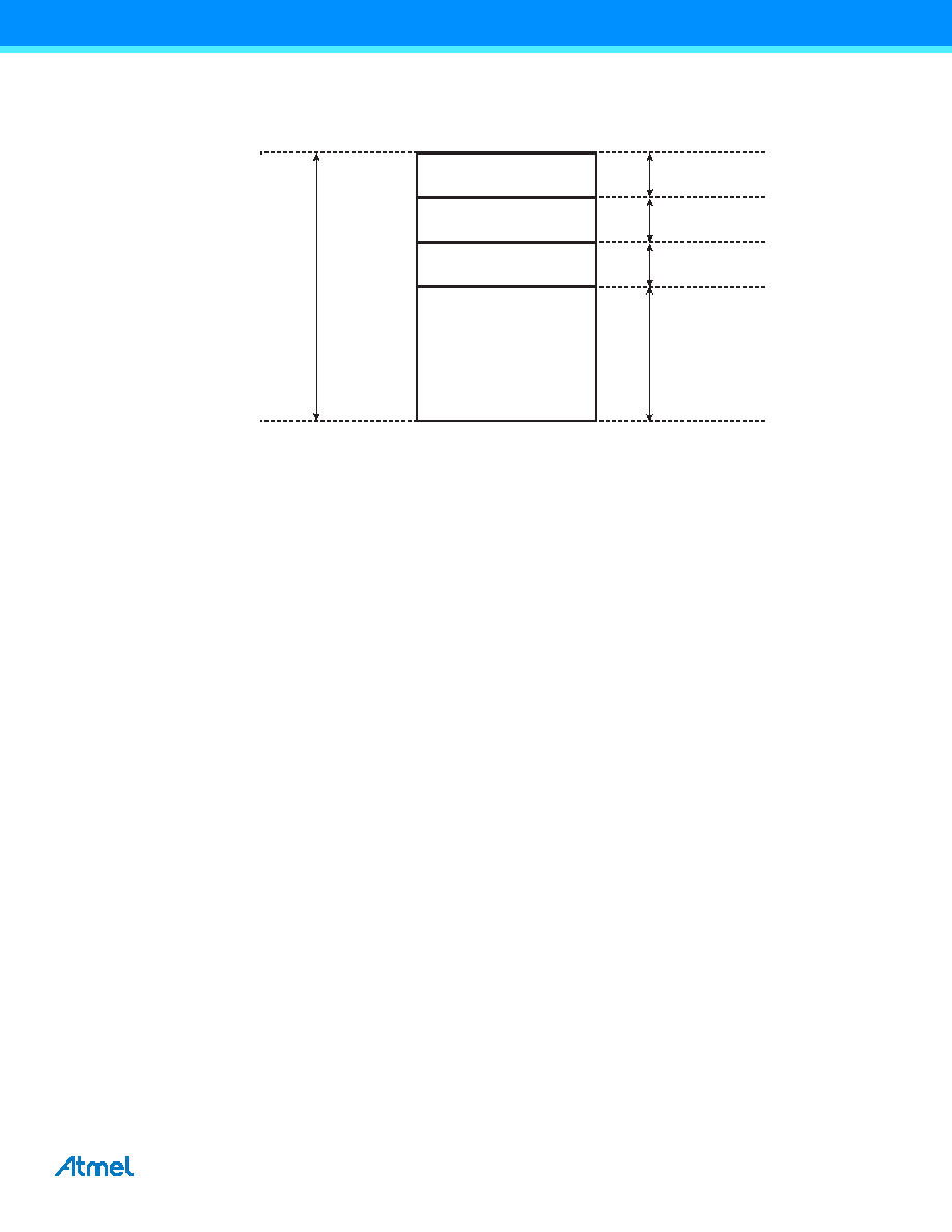
Figure 18-3. Internal Memory Mapping
18.3.2.2
Internal Memory Area 0
The first 32 bytes of Internal Memory Area 0 contain the ARM processor exception vectors, in particular, the Reset
Vector at address 0x0.
Before execution of the remap command, the on-chip Flash is mapped into Internal Memory Area 0, so that the
ARM7TDMI reaches an executable instruction contained in Flash. After the remap command, the internal SRAM at
address 0x0020 0000 is mapped into Internal Memory Area 0. The memory mapped into Internal Memory Area 0 is
accessible in both its original location and at address 0x0.
18.3.3
Remap Command
After execution, the Remap Command causes the Internal SRAM to be accessed through the Internal Memory
Area 0.
As the ARM vectors (Reset, Abort, Data Abort, Prefetch Abort, Undefined Instruction, Interrupt, and Fast Interrupt)
are mapped from address 0x0 to address 0x20, the Remap Command allows the user to redefine dynamically
these vectors under software control.
The Remap Command is accessible through the Memory Controller User Interface by writing the MC_RCR
(Remap Control Register) RCB field to one.
The Remap Command can be cancelled by writing the MC_RCR RCB field to one, which acts as a toggling com-
mand. This allows easy debug of the user-defined boot sequence by offering a simple way to put the chip in the
same configuration as after a reset.
18.3.4
Abort Status
There are three reasons for an abort to occur:
access to an undefined address
an access to a misaligned address.
When an abort occurs, a signal is sent back to all the masters, regardless of which one has generated the access.
However, only the ARM7TDMI can take an abort signal into account, and only under the condition that it was gen-
erating an access. The Peripheral DMA Controller does not handle the abort input signal. Note that the connection
is not represented in Figure 18-1.
256M Bytes
Internal Memory Area 0
Undefined Areas
(Abort)
0x0000 0000
0x000F FFFF
0x0010 0000
0x001F FFFF
0x0020 0000
0x002F FFFF
0x0FFF FFFF
1M Bytes
253M bytes
Internal Memory Area 1
Internal Flash
Internal Memory Area 2
Internal SRAM
0x0030 0000
发布紧急采购,3分钟左右您将得到回复。
相关PDF资料
52559-2270
CONN FFC 22POS .5MM VERT ZIF SMD
52559-1870
CONN FFC 18POS .5MM VERT ZIF SMD
DSPIC33EP64MC506-I/PT
IC DSC 16BIT 64KB FLASH 64TQFP
52745-1896
CONN FFC 18POS .5MM R/A ZIF SMD
PIC16LC622-04/P
IC MCU OTP 2KX14 COMP 18DIP
PIC16LF84A-04/P
IC MCU FLASH 1KX14 EE 18DIP
DSPIC30F1010-30I/MM
IC DSPIC MCU/DSP 6K 28QFN
52745-1696
CONN FFC 16POS .5MM R/A ZIF SMD
相关代理商/技术参数
PIC16C63A-04I/SP
功能描述:8位微控制器 -MCU 7KB 192 RAM 22 I/O RoHS:否 制造商:Silicon Labs 核心:8051 处理器系列:C8051F39x 数据总线宽度:8 bit 最大时钟频率:50 MHz 程序存储器大小:16 KB 数据 RAM 大小:1 KB 片上 ADC:Yes 工作电源电压:1.8 V to 3.6 V 工作温度范围:- 40 C to + 105 C 封装 / 箱体:QFN-20 安装风格:SMD/SMT
PIC16C63A-04I/SS
功能描述:8位微控制器 -MCU 7KB 192 RAM 22 I/O RoHS:否 制造商:Silicon Labs 核心:8051 处理器系列:C8051F39x 数据总线宽度:8 bit 最大时钟频率:50 MHz 程序存储器大小:16 KB 数据 RAM 大小:1 KB 片上 ADC:Yes 工作电源电压:1.8 V to 3.6 V 工作温度范围:- 40 C to + 105 C 封装 / 箱体:QFN-20 安装风格:SMD/SMT
PIC16C63A04SP
制造商:MICROCHIP 功能描述:NEW
PIC16C63A-20/SO
功能描述:8位微控制器 -MCU 7KB 192 RAM 22 I/O RoHS:否 制造商:Silicon Labs 核心:8051 处理器系列:C8051F39x 数据总线宽度:8 bit 最大时钟频率:50 MHz 程序存储器大小:16 KB 数据 RAM 大小:1 KB 片上 ADC:Yes 工作电源电压:1.8 V to 3.6 V 工作温度范围:- 40 C to + 105 C 封装 / 箱体:QFN-20 安装风格:SMD/SMT
PIC16C63A-20/SP
功能描述:8位微控制器 -MCU 7KB 192 RAM 22 I/O RoHS:否 制造商:Silicon Labs 核心:8051 处理器系列:C8051F39x 数据总线宽度:8 bit 最大时钟频率:50 MHz 程序存储器大小:16 KB 数据 RAM 大小:1 KB 片上 ADC:Yes 工作电源电压:1.8 V to 3.6 V 工作温度范围:- 40 C to + 105 C 封装 / 箱体:QFN-20 安装风格:SMD/SMT
PIC16C63A-20/SP
制造商:Microchip Technology Inc 功能描述:8 Bit Microcontroller Clock Speed:20MHz
PIC16C63A-20/SS
功能描述:8位微控制器 -MCU 7KB 192 RAM 22 I/O RoHS:否 制造商:Silicon Labs 核心:8051 处理器系列:C8051F39x 数据总线宽度:8 bit 最大时钟频率:50 MHz 程序存储器大小:16 KB 数据 RAM 大小:1 KB 片上 ADC:Yes 工作电源电压:1.8 V to 3.6 V 工作温度范围:- 40 C to + 105 C 封装 / 箱体:QFN-20 安装风格:SMD/SMT
PIC16C63A-20E/SO
功能描述:8位微控制器 -MCU 7KB 192 RAM 22 I/O RoHS:否 制造商:Silicon Labs 核心:8051 处理器系列:C8051F39x 数据总线宽度:8 bit 最大时钟频率:50 MHz 程序存储器大小:16 KB 数据 RAM 大小:1 KB 片上 ADC:Yes 工作电源电压:1.8 V to 3.6 V 工作温度范围:- 40 C to + 105 C 封装 / 箱体:QFN-20 安装风格:SMD/SMT